Overview
This article provides a summary of ECP5UM features and capabilities as applied to the Private Island ® project and Darsena development board. Official Lattice documentation takes precedence whenever conflicts occur.
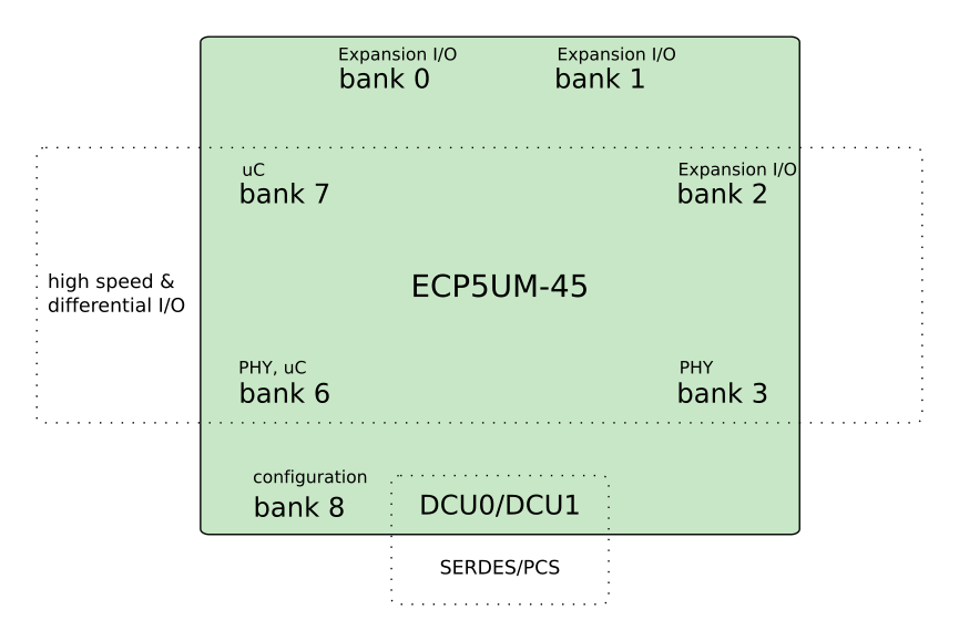
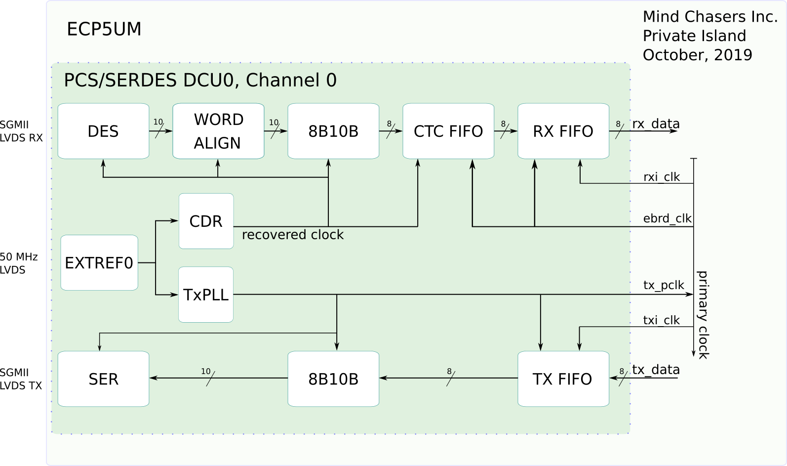
The ECP5UM includes a hard four-port PCS/SERDES block, which is used on Darsena for connectivity to two on-board SGMII Ethernet PHYs and two expansion slots. We document our use of this block here.
The distinctions between the ECP5UM and ECP5 are the aforementioned PCS/SERDES block and the requirement to use a paid Lattice Diamond license with the ECP5UM. However, there is the potential to use the Yosys open source toolchain with both devices.
Although Darsena utlizes SGMII PHYs and the ECP5UM, we are investigating supporting RGMII PHYs with the ECP5 utilizing DDR I/O. Therefore, DDR technology is discussed below with this future use in mind.
The text below applies to both the ECP5 and ECP5UM unless specified otherwise.
ECP5(-45) Basics
- FPGA Device: LFE5UM-45-8BG381C
- 381-pin BGA
- 40 nm process
- 44K LUTs (8 LUTs per PFU, 2 LUTs per slice)
- 108 sysMem EBR blocks (18 kbit each). Total system EBR: 1944 kbit. Rows 10, 34, and 58
- Distributed memory, which utilizes the LUTs
- Two rows of DSP slices.
- Four Delay Locked Loops (DLLs) and Four Phase Locked Loops (PLLs).
- Left and right banks are tuned for high speed interfaces and differential signaling & clocks: 7 & 6 are left and 2 & 3 are right. These banks are referred to as "high-speed banks" below. Banks 0 & 1 are on top. Bank 8 (sysConfig) and SERDES/PCS are on bottom. These positions are relative to the A1 ball being in the upper left hand corner of the device.
PFU
- Each PFU has 4 slices, 53 inputs, and 25 outputs
- Each PFU has 8 LUTs (16*2*8 = 256 bits).
- Each LUT can be configured as a 16x2 bit memory.
- Each slice has two LUT4 lookup tables, so each PFU has eight LUT4s.
- A PLC is a subset of a PFU and is defined as four slices.
ECP5 General References
- ECP5 Product Page
- TN1269 ECP5 HW Checklist
- TN1074 PCB Layout
- TN1033 High-Speed PCB Design Considerations
sysIO (ECP5 system I/O)
sysIO Overview:
- SysIO buffers are either ratioed or referenced ( referenced to VREF ). A ratioed buffer can be referenced from VCCIO or another rail (e.g, VCC is also used to power the 1.2V (LVCMOS12) ratioed buffers so these can be captured independently of VCCIO ).
- Each PIC includes 4 PIOs (A,B,C,D) on left and right banks and 2 PIOs on top and bottom banks (A, B)
- Each bank has a dedicated VCCIO supply voltage. IO signaling from 1.2V to 3.3V is supported.
- VCCAUX (2.5V) powers all the differential and referenced input buffers.
- VCCIO powers the single ended outputs.
- Each PIO includes a sysIO buffer and I/O logic (IOLOGIC). The I/O logic includes input, output and tri-state registers that implement both single data rate (SDR) and double data rate (DDR) applications along with the necessary clock and data selection logic.
- Single-ended signaling can be divided into two types: internal ratioed and external reference. The former relies on the proper VCCIO voltage level. The latter relies on a reference voltage (VREF).
- All differential and referenced inputs are independent of VCCIO . When an output is configured as an open drain, it can also be placed independent of VCCIO.
- VREF: The high-speed banks (2, 3, 6, and 7) each have a voltage reference input pin (VREF) to support referenced signaling, such as SSTL (Stub Series Terminated Logic). The VREF voltage is used to set the threshold for the referenced input buffers, such as SSTL The VREF pins are: B2 (bank 7), K5 (bank 6), P16 (bank 3), and D20 (bank 2).
- Single-ended output buffers and some ratioed input buffers (LVTTL and LVCMOS) are powered using VCCIO. LVTTL, LVCMOS33, LVCMOS25 and LVCMOS12 can also be set as fixed threshold inputs independent of VCCIO.
- The left/right side also have one LVDS output driver per four IOs and one differential termination resistor per two IOs.
sysIO LVDS
- 50% of the PIO pairs on the left and right banks of the device can be configured as LVDS transmit pairs (A/B pair), and all pairs on left and right can be configured as LVDS receive pairs.
- For the high-speed banks, each PIO pair supports a true LVDS differential input buffer. However, only the PIO A, B pair supports a true LVDS differential output buffer. Each A/B and C/D pair supports programmable on/off differential input termination of 100 ohms.
- 100 ohm differential termination is supported but only one termination setting can be used per bank. The termination tolerance is +/- 20%
- Regardless of bank, two adjacent PIOs can also be used to provide a complementary output driver pair.
Delay Lines
- A static (DELAYG) or dynamic (DELAYF) delay line can be applied within each IOLOGIC cell; however, only one delay can be applied within each cell (either input or output direction).
- Using DELAYF, you can overwrite the DELAY setting dynamically using the MOVE and DIRECTION control inputs. The LOADN resets the delay back to the default value.
- The delay is in ~25 ps increments
sysIO References
- TN1262 ECP5 sysIO Usage Guide
- TN1265 ECP5 High Speed I/O Interface
sysClock
ECP5 sysClock Basics
- 16 primary clocks per each of the four ECP5UM quadrants
- Max of 60 unique clock input sources (PLLs, External Inputs, SERDES, etc.)
- By default: each clock is routed to all quadrants. However, Diamond preference can be used to specify quadrant.
- There are two Edge Clock (ECLK) networks per bank IO on the Left and Right sides of the devices.
- Clock elements:
- primary clocks (16 per each quadrant). Maximum of 60 different inputs can be routed / switched to primary clock lanes.
- edge clocks
- Two per bank on left and right side for a total of eight
- Edge Clock Sources:
- PCLK pins
- DLLDEL
- PLL Outputs (Only the PLL CLKOP and CLKOS outputs can go to the ECLK network)
- ECLK bridge
- Internal nodes
- Edge Clock Dividers (4) (CLKDIVF)
- Edge Clock Bridge with Clock Select (2) (ECLKBRIDGECS)
- Edge Clock Stop (ECLKSYNCB), one for each edge clock (8)
- PLLs (4).
- There are six GPLL input pairs (T/C):
- Two in each of the top corners: ULC_GPLL (bank 7: A4, A5), (bank 0: A6, B6), URC_GPLL (bank 2: C18,D17), (bank1: A19, B20)
- One in each bottom corner:LLC_GPLL (bank 6: P3, P4), LRC_GPLL (bank 3: U16, T17)
- All four PLL outputs can go to the Primary Clock network. Only CLKOP and CLKOS can go to the ECLK network.
- Input PLL Clock Selection (PLLREFCS). The dedicated PLL inputs are routed to the input of the PLLREFCS components
- There are six GPLL input pairs (T/C):
- DDRDLL (4) is a dedicated DLL for creating the 90° clock delay for DDR memory and High Speed IO interfaces.
- an internal oscillator (OSCG) used for control logic state machines
- clock dividers (4)
- Dynamic Clock Select (2) (DCSC), select between two independent clock sources to the primary clock network
- General routing PCLK Pins: Some Dedicated pins (GR_PCLK) can access some CIBs along the edge of the device and can drive the primary clock routing from this CIB. These will go through some general routing but have direct access to the primary clock from this dedicated CIB. There are four at the left side and right side, four at the top side of the device. These pins can be used when user runs out of PCLK pins.
Sysclock PLL Notes
- The CLKOP, CLKOS, CLKOS2, and CLKOS3 outputs can all be used to drive the primary clock network.
- Only CLKOP and CLKOS outputs can go to the edge clock network.
Primary Clocks
- Dedicated PCLK clock pins are used to route an external clock source to FPGA logic and I/O.
- 12 PCLK diff pin pairs: banks 0, 1, 2, 3, 6, and 7. Note that
bank 8 doesn't have PCLK PIO.
- bank 0: PCLK0_0 (B11, C11), PCLK0_1 (A10, A11)
- bank 1: PCLK1_0 (B12, C12), PCLK1_1 (D11, E11)
- bank 2: PCLK2_0 (J20, K20), PCLK2_1 (J19, K19)
- bank 3: PCLK3_0 (L19, M19), PCLK3_1 (L20, M20)
- bank 6: PCLK6_0 (H2, G1), PCLK6_1 (G2, F1)
- bank 7: PCLK7_0 (F2, E2), PCLK7_1 (G3, F3)
- Primary Clock Sources:
- Dedicated Clock Pins
- PLL Outputs
- CLKDIV Outputs
- Internal FPGA Fabric Entries
- SERDES/PCS clocks
- OSCG
Edge Clocks
- There are two edge clocks per high speed bank (left and right sides).
- There is one ECLK Mux per side (two per device). This drives the two edge clocks for each bank.
PLL
- Only CLKOP and CLKOS can go to the ECLK network.
- PLLs have dedicated PLL input pins that are not Primary Clock input pins
ECP5 sysClock References
- TN1263 sysClock PLL/DLL Usage Guide
System Memory (sysMEM)
sysMem Overview
- 108 sysMem blocks (18 kbit each)
- 108*18k = 1944 K
- The EBR consists of an 18 Kb RAM with memory core, dedicated input registers and output registers with separate clock and clock enable. Each EBR includes functionality to support true dual-port, pseudo dual-port, single-port RAM, ROM and FIFO buffers (via external PFUs).
- EBRs are used extensively throughout the design as FIFOs and true DPRAMs and are typically instantiated as a 2k x 9-bit block.
sysMem references
ECP5 System Configuration (sysConfig)
Supported sysConfig Modes
- 1149.1 JTAG to program the ECP5 directly
- Master (MSPI) for ECP5 to boot from ROM
sysConfig I/O
- PROGRAMN (FPGA_PGM#, INPUT)
- INITn (bidirectional, open-drain), asserts low to indicate the SRAM configuration memory is being erased. Returns high to indicate device is ready for programming. Subsequent assertion by the device indicates an error during programming
- DONE (bi-directional, open drain with a weak pull-up) is asserted when FPGA enters user mode. DONE can be asserted externally to hold off entering user mode.
- MOSI: For MSPI, MOSI is an output
- MISO: For MSPI, MISO is an input
sysConfig Basics
- Max uncompressed image of ~9.74Mb
- INITN is asserted by ECP5 to indicate the SRAM is being erased. When it goes high, it indicates that the ECP5 is ready to read in its config bits from FLASH. If INITN again goes low, this indicates an error with the configuration process.
- When the device is programmed through IEEE 1149.1 JTAG control, the sysCONFIG programming pins, such as DONE, cannot be used to determine programming progress.
- During configuration the user-programmable I/Os are tristated with an internal pull-down resistor enabled . If any pin is not used (or not bonded to a package pin), it is tristated and it defaults to pull-down enabled after configuration.
MSPI
- Diamond flow only generates default sub-mode bitstream, which is serial and slow read.
- To change to a different sub-mode, you must alter the bitstream using Lattice Deployment Tool.
- Can instantiate USRMCLK macro to use MSPI in user mode.
sysConfig References
- TN1260 sysConfig Usage Guide
- TN1215 Security Encryption Key Programing Guide
- TN1216 Dual and Multiple Boot
- TN1087 Minimizing System Interruption During Configuration Using TransFR Technology
DSP Functionality (sysDSP)
To be added...
SysDSP References
ECP5 Power
Power Summary
- Power up
- it is recommended that the I/O buffers be powered-up prior to the FPGA core fabric. VCCIO supplies should be powered-up before or together with the VCC and VCCAUX supplies.å
- it is required to ramp VCCIO8 above VIH of the external SPI Flash, before at least one of the other two supplies (VCC and/or VCCAUX) is ramped to VPORUP voltage level . For safe measure, consider keeping either PROGRAMN or INITN pin LOW during power up
- It is required to power up VCCA, before VCCAUXA is powered up.
- VCCAUX: Auxiliary power supply pin. This dedicated pin powers
all the differential and referenced input buffers. VCCAUX = 2.5 V.
- LVDS inputs use LVDS comparator, which uses VCCAUX power
- VCCAUX ramp rate must not exceed 30 mV/us during power-up when transitioning between 0 V and 3 V.
- VCCAUXA: SERDES Auxiliary Supply Voltage
- VCCA:
- ECP5UM devices require 1.1 V on VCCA, VCCHRX and VCCHTX supplies.
- For an unused channel in a Dual, it is advised to connect the VCCHTX to VCCA, and user can leave VCCHRX unconnected (p 40 of DS)
- ECP5UM devices require 1.1 V on VCCA, VCCHRX and VCCHTX supplies. ECP5-5G devices require 1.2 V on these supplies
- During power-up and power-down sequences, the I/Os remain in tristate until the power supply voltage is high enough to ensure reliable operation
- Unused I/O:
- The GPIO of the device at power-up will default to tri-stated outputs with active weak input pull-downs
- GPIO not defined in the user design will remain output tri-stated and the input will have a weak pull-down enabled.
ECP5 Power Pins
- VCC: Powers the core and is available for ratioed buffers.
- VCCIO: Powers the single ended I/O, separate for each bank.
- VCCAUX: Auxiliary power supply pin. This dedicated pin powers the differential and (SSTL)referenced input buffers. Bank VCCAUX is also used to power the push-pull output pre-driver sections. (Pg 6 sysio): "Some of the ratioed buffers are powered by VCCAUX". (Pg 6 of sysio): "VCCAUX (2.5 V), supports hysteresis, and is used for 3.3 V and 2.5 V signaling."
- VREF: Reference supply pins for I/O bank x. Pre-determined shared pin in each bank are assigned as VREF1 input. When not used, they may be used as I/O pins.
- VCCAx : SERDES, transmit, receive, PLL and reference clock buffer power supply for SERDES Dual x. All VCCA supply pins must always be powered to the recommended operating voltage range. If no SERDES channels are used, connect VCCA to VCC. VCCAx = 1.1 V for ECP5, VCCAx = 1.2 V for ECP5-5G.
- VCCAUXAx : SERDES Auxiliary Power Supply pin for SERDES Dual x. VCCAUXAx = 2.5 V.
- VCCHRX : SERDES High-Speed Inputs Termination Voltage Supplies. These pins should be powered to 1.1 V on ECP5
- VCCHTX : SERDES High-Speed Outputs Buffer Voltage Supplies. These pins should be powered to 1.1 V on ECP5
ECP5 Power References
Miscellaneous
- The ECP5 has a Digital Temperature Readout module to measure the operating junction temperature.
Acronyms and Terms
- CIB: common interface block, which is a switch matrix that can be programmed to connect virtually any routing resource to any input or output of the logic element.
- DCC: Dynamic Clock Control
- DCS: Dynamic Clock Select
- DCU: SERDES Dual Channel Unit
- EBR: Embedded Block RAM (sysMEM)
- ECLK: Edge Clock
- IOL: I/O Logic Block ( logic at the I/O buffer )
- LPF: (logic preference file) holds pin out
- LSR: Local Set / Reset, programmable as synchronous/ asynchronous)
- NCD: native circuit description
- NGD: native generic database ( output of synthesis and represents logical design )
- PAR: Placement and Routing ( *.prf file is the input )
- PCLK: Primary Clock
- PFU: Programmable Functional Unit
- PIC: Programmable Interface Cell. PIOs. PICs provide high-speed registers and buffering.
- PIO: Programmable I/O Cell, programmable logic associated with an I/O
- PLC: Programmable Logic Cell ( has four slices, etc. )
- PMI: Parameterized Module Instantiation, see Using PMI
- PRF File: Physical Preferences ( output of MAP )
- SCI: SERDES Client Interface
- SCLK: Primary Clock
- VCD: value change dump


