Overview
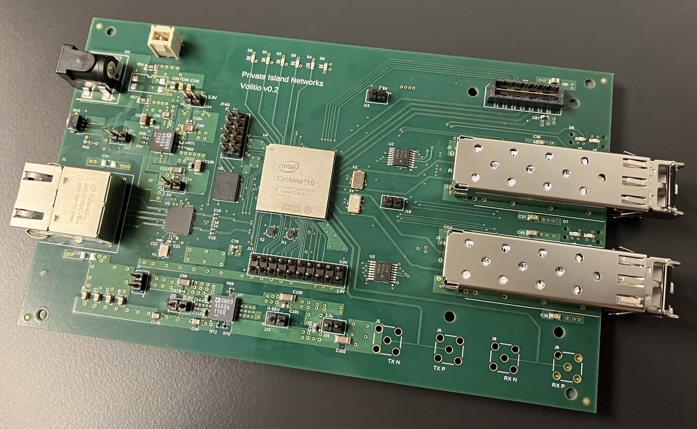
Meet our Volitio™ board, our 10G capable system designed for Private Island ® that utilizes the Intel Cyclone 10 GX. This FPGA is a very powerful device that provides 10 Gbps network connectivity using embedded high-speed transceivers. We utilize this high-performance system to develop custom networking and bridging solutions for our customers.
This article documents various board and FPGA features that are relevant to Private Island specifically and networking & embedded computing in general. This article is a work in process and will be updated periodically.
The Intel Cyclone 10 GX
Breaking Down the Part Number 10CX085YU484I5G:
- X: 12.5 Gbps transceivers
- 085: 85K Logic Elements (LE)
- Y: 0.9 V Core Voltage
- U: Ultra FineLine BGA (UBGA) 0.8 mm pitch, 484 ball, 19 mm x 19 mm package
- I: Industrial
- 5: (fastest)
- G: ROHS
Features and Resources of the 10CX085YU484I5G:
- 188 GPIO (70 true LVDS)
- Four I/O banks: 2L (3V) and 2K, 2J, & 2A (1.8V LVDS)
- Each I/O bank contains one I/O PLL and ~48 GPIOs
- 84 LVDS pairs (Each LVDS I/O pair can be used as differential input or output)
- LVDS data rate up to 1.434 Gbps
- Six high-speed transceivers (single bank) with two input clocks
- Two (fractional) fPLLs
- 31,000 ALMs
- 291 (5,820 Kb) M20K memory blocks
- 1,044 (653 Kb) MLAB memories
- 84 DSP blocks (168 18x19 multipliers)
Other notes to keep in mind
- Fabricated using a 20 nm process
- Internal pull ups & downs are 25K
- Maximum fabric frequency is 350 MHz.
- "High Speed Differential I/O" is the dedicated I/O standard for the transmitter in Intel Cyclone 10 GX transceivers.
- Uncompressed Configuration Bit Stream Size (bits): 81,923,582
- Cyclone 10 GX and Cyclone 10 LP have virtually nothing in common from a hardware viewpoint
- One LUT level can generally implement a function of 6 inputs
- Top view of the silicon die corresponds to a reverse view of the device package.
Cyclone 10 GX Power Rails
| Name | Voltage | Description | Group | Notes |
|---|---|---|---|---|
| VCC | 0.9 | Core | 1 | |
| VCCP | 0.9 | Periphery circuitry and transceiver fabric interface | 1 | |
| VCCERAM | 0.9 | Embedded memory | 1 | |
| VCCT_GXB[L1][C,D] | 0.95 | Transmitter | 1 | |
| VCCR_GXB[L1][C,D] | 0.95 | Receiver | 1 | |
| VCCH_GXBL | 1.8 | Transceiver output buffer | 2 | |
| VCCPGM | 1.8 | Configuration pins | 3 | Configure for 1.8V ROM |
| VCCBAT | 1.8 | Battery back-up | N/A | For the device to exit POR, you must power the VCCBAT power supply even if you do not use the volatile key. |
| VCCPT | 1.8 | programmable power technology and I/O pre-driver | 2 | |
| VCCA_PLL | 1.8 | PLL analog voltage regulator | 2 | |
| VCCIO | 3V and 1.8V | I/O buffers | 3 | |
| VREFP_ADC | 1.25 | Precision voltage reference for voltage sensor | ? |
Miscellaneous Notes Regarding Power and Power Sequencing
- The following power supply rails are not monitored by the POR circuit: VCCH_GXB, VCCR_GXB, VCCT_GXB, VCCA_PLL
- VCCBAT does not have any sequence requirements.
- The Group 3 1.8V power rails can be ramped up with the Group 2 1.8V power rails
- During the power-up/down sequence, the device output pins are tri-stated.
- Fully configure the transceiver block before driving or having any activity on the transceiver pins.
- Cyclone 10 GX devices do not support hot socketing except under some specific conditions.
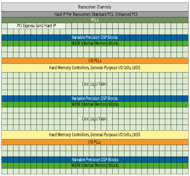
High Level Block Diagrams
The next few figures are taken from either the Intel Cyclone 10 GX Fabric and General Purpose I/Os Handbook or the Transceiver PHY User Guide.
The figure below shows the layout of I/O banks along with the transceiver block (column 1). Note that the 85K LE device has one block with six transceivers.

The figure below shows the Cyclone 10 GX resource layout that includes PLLs, memories, DSPs, etc.
The next figure shows a block diagram of the transceiver bank/block. Intel encourages the developer to use the ATX PLL whenever possible to achieve the lowest jitter.
The transceiver bank has two high-speed reference clock inputs: REFCLK_GXBL1C_CHT and REFCLK_GXBL1C_CHB (1C column).

Additional notes regarding the transceiver block:
- Unlike the ATX PLL, the fPLL can be used to synthesize frequencies that can drive the core through the FPGA fabric clock networks.
- The channel PLLs of channel 1 and 4 can be used as transmit PLLs when configured in clock multiplier unit (CMU) mode.
- Each transceiver channel has a local CGB. The local CGB is used for dividing and distributing non-bonded clocks to its own PCS and PMA blocks.
- PCS blocks support continuous data rates between 1.0 Gbps and 10.81344 Gbps.
- The channel PLLs of channel 1 and 4 can be used as transmit PLLs when configured in clock multiplier unit (CMU) mode.
- Each transceiver channel has a local CGB. The local CGB is used for dividing and distributing non-bonded clocks to its own PCS and PMA blocks.
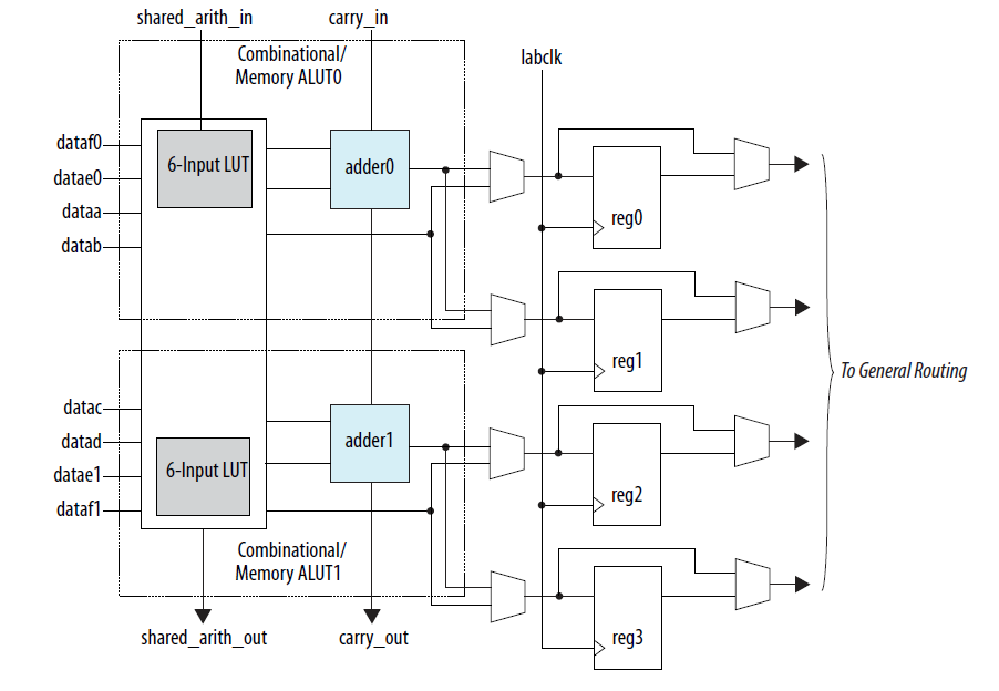
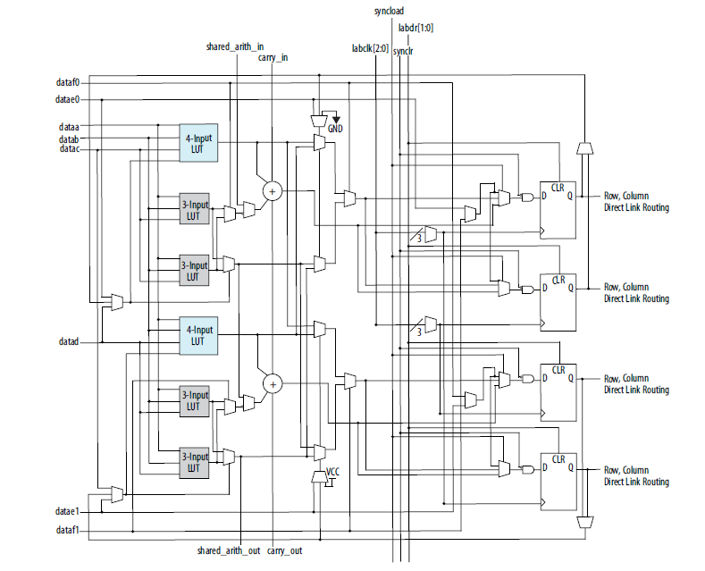
LABs and ALMs
- Each LAB consists of 10 ALMs and one LAB Control Block
- Each ALM has two LUTs
- Two LUTs can be used together to implement a single logic equation of up to 7 inputs or independently to implement two logic functions of up to 6 inputs.
- An ALM can also be configured to implement a 32x2, 64-bit memory
Memory
There are two types of embedded memory withn the Cyclone 10 GX:
- 20 Kb M20K blocks that are dedicated memory resources.
- 640 bit Memory Logic Array Blocks (MLABs). Each MLAB is made up of ten adaptive logic modules (ALMs). These can be configured as ten 32 x 2 blocks, providing one 32 x 20 simple dual-port SRAM block per MLAB.
M20K Notes
- Unused M20K blocks are set to sleep mode by disabling VCCERAM to reduce static power.
MLAB Notes
- Quartus sets unused MLABs to low power mode to reduce static power.
DSP Blocks
To Be Added
More Coming...
We will be adding more information pertaining to memory, DSP blocks, I/O buffers, etc.
Terms
- Register packing: improves device utilization by allowing unrelated register and combinational logic to be packed into a single ALM
Acronyms
- ASx4: 4-bit Active Serial
- ALM: Adaptive Logic Modules
- AS: Active Serial (Configuration)
- ATX: Advanced Transmit (PLL). The ATX PLL is the transceiver channel's primary transmit PLL.
- BER: Bit Error Ratio
- CTLE: Continuous Time Linear Equalization
- CDR: clock data recovery
- DFE:Decision Feedback Equalization
- CGB: Clock Generation Block
- CMU: Clock Multiplier Unit (PLL)
- CvP: Configuration Via Protocol
- DCM: Distributed Clock Mux
- DPA: Dynamic Phase Alignment
- fPLL: Fractional PLL
- FPP: Fast Passive Parallel configuration mode
- GCLK: Global Clock Network
- HPS: Hard Processor System
- HSSI: high-speed serial interface
- HSTL: High-Speed Transceiver Logic
- IOCSR: I/O configuration shift register
- IOE: I/O Element
- JIC: JTAG Indirect File
- LAB: Logic Array Block, which consists of ALMs
- LPM: Library of Parameterized Modules
- LR: Long Reach (backplane)
- MLAB: Memory LAB
- OCT: On-chip Termination
- OpenCL: Open Computing Language
- PCLK:Periphery Clock Network
- PFD: Phase Frequency Detector
- PFL: Parallel Flash Loader
- PLL: Phase Lock Loop
- PIPE: PHY Interface For the PCI Express, SATA, USB 3.1, DisplayPort, and USB4 Architectures
- POR: Power On Reset
- PPMC: Programmable Power Management Controller
- PS: Passive Serial (Configuration)
- SERDES: serializer / deserializer
- SCLK: Section Clock
- SFL: Serial Flash Loader
- SOF: SRAM Object File
- STAPL: Standard Test and Programming Language
- SR: Short Reach (chip-to-chip)
- RCLK: Regional Clock Network
- SCLK: Section Clock
- TRS: Transceiver Reset Sequencer
- TREs: Transceiver Reset Endpoints
- TSD: Temperature Sensing Diode
- VCCPT: Pre-Driver Voltage
- VCD: Value Change Dump (file)
Cyclone 10 GX References
- Device Overview
- Device Errata and Design Guidelines
- Clock Control Block (ALTCLKCTRL) IP Core
- PHY Interface For the PCI Express, SATA, USB 3.1, DisplayPort, and USB4 Architectures
- Cyclone 10 GX XCVR Toolkit Reference Design
- Pin-out files for Intel FPGAs
- Cyclone® 10 GX Device Family Pin Connection Guidelines
- Webinar: Transceiver Basics
- Support Resources : Board Design


