Overview
In this article, we review the Serial Peripheral Interface (SPI) protocol in the context of the Private Island FPGA-based open source network processor using the Darsena development board. SPI is a full duplex, synchronous, serial protocol that utilizes a four wire interface:
- SCLK: Serial Clock driven by the master. For Darsena, this is an NXP K02 microcontroller (µC).
- MOSI: Master Out / Slave In. K02 drives the data, and the FPGA receives it.
- MISO: Master In / Slave Out. FPGA drives the data.
- PCS / SS: Peripheral Chip Select / Slave Select. K02 asserts this wire to signal to the FPGA that an SPI cycle is underway.
The interface supports a single master and multiple slaves, where each slave is selected by a separate chip select (PCS/SS). Each transfer is full duplex on the hardware bus (software protocol need not be full duplex).
SPI supports 4 modes, which are configured by two parameters: CPOL and CPHA
- CPOL: Clock Polarity designates the signal level of SCLK when the bus is idle. CPOL=0 corresponds to SCLK being low to indicate an idle bus.
- CPHA: Clock Phase determines which edge of SCLK is sampled (rising or falling). CPHA=0 indicates data is captured on the rising edge of SCLK and driven on the following falling edge. Note that the first data bit is output on the assertion SS.
SPI defines the hardware protocol but not a software protocol. Therefore, the master and slave must agree to the higher-level protocol used (e.g., the meaning of each byte and bit).
Project Implementation Specifics
- SPI is utilizied by the external µC to access various internal memory blocks of the FPGA, and the protocol is depicted in Figure 1 below.
- 9-bit word transfers are utilized to match the 9-bit DPRAMs instantiated inside the FPGA.
- Since the FPGA is the slave, SCLK is asynchronous to the internal FPGA controller clock and is sampled internal to the FPGA by the higher frequency internal clock.
- Maximum SPI clock rate is TBD, limited by the K02 specifications, and must be TBD times less than the FPGA clock used to sample it.
- Each SPI cycle is terminated by negation of slave select.
K02 SPI Configuration
Listed below is the default SPI configuration of the K02:
- Bit rate: 1MHz
- CPOL = 0 (kDSPI_ClockPolarityActiveHigh)
- CPHA = 0 (kDSPI_ClockPhaseFirstEdge)
- MSB first (kDSPI_MsbFirst)
- 9-bit transfers (bitsPerFrame = 9)
SPI Data Protocol
Figure 1 shows the protocol for an SPI Write and an SPI Read. The µC always transmits on the MOSI wire a device address, RWN indication, and memory address as the first two words. The FPGA always transmits on the MISO wire 0x76 to start each SPI exchange.
During writes, the µC continues to write words as a burst with the FPGA automatically incrementing the address and indicating the last address written via Word Count on the MISO wire. Wrap around is target memory specific within the FPGA.
A full duplex data exchange is in development to provide for efficient packet transfer to and from the µC Ethernet MAC data buffers within the FPGA.
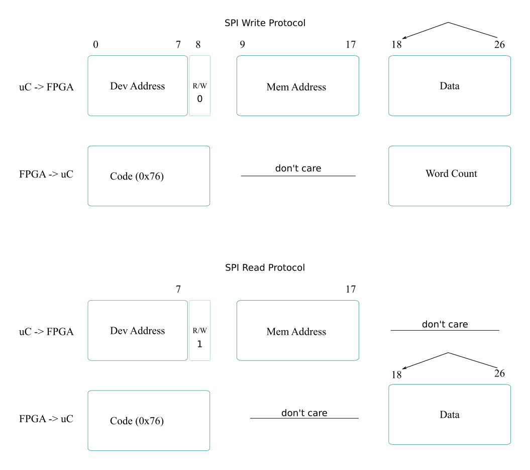
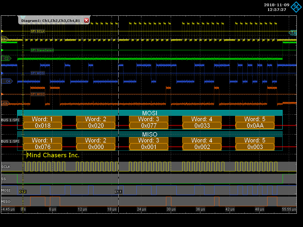
Figure 2 shows a scope trace of an SPI write of three words using the following parameters:
- Device Address: 0xc (µC TX buffer)
- R/W: 0
- Mem Address: 0x020
- data written: 0x077, 0x033, 0x0AA
Note that the data is transmitted as 9-bit words and begins when SS is driven low (green trace). MOSI is the blue trace, and MISO is the orange trace.