Overview
This article documents the Verilog Serial Peripheral Interface (SPI) module for Private Island. This is a slave-only implementation that is used primarily to transfer data between internal FPGA memories and an external micro controller (µC).
The project's source code is hosted here using cgit, and here is a link to spi.v.
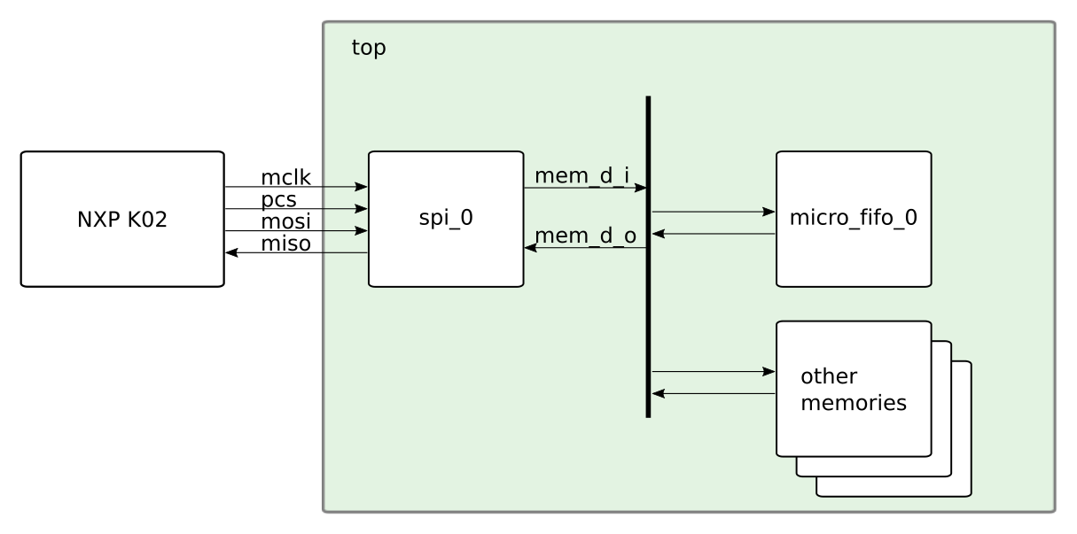
Private Island is an open source FPGA-based network processor for Gigabit Ethernet network security, IoT, and control applications. The figure below depicts how SPI is utilized on the Darsena development board. An NXP K02 µC is an external ARM Cortex M4 processor, and it accesses the FPGA's internal memories via SPI. The K02 is the SPI master and drives the clock (mclk), chip select (pcs), and Master Out / Slave In (mosi) signals. For additional information on SPI and the protocol used on Private Island, please see SPI Basics and Protocol.
The overall FPGA implementation consists of many open source modules, which are mainly instantiated in the top level module top. The description and figures below discuss accessing the transmit (TX) buffer in the micro_fifo_0 module, and this description also applies to the other memory blocks.
The mem_d_i and mem_d_o buses are declared in the top module and are used to route data into and out of the memories via the spi module.
Module Description
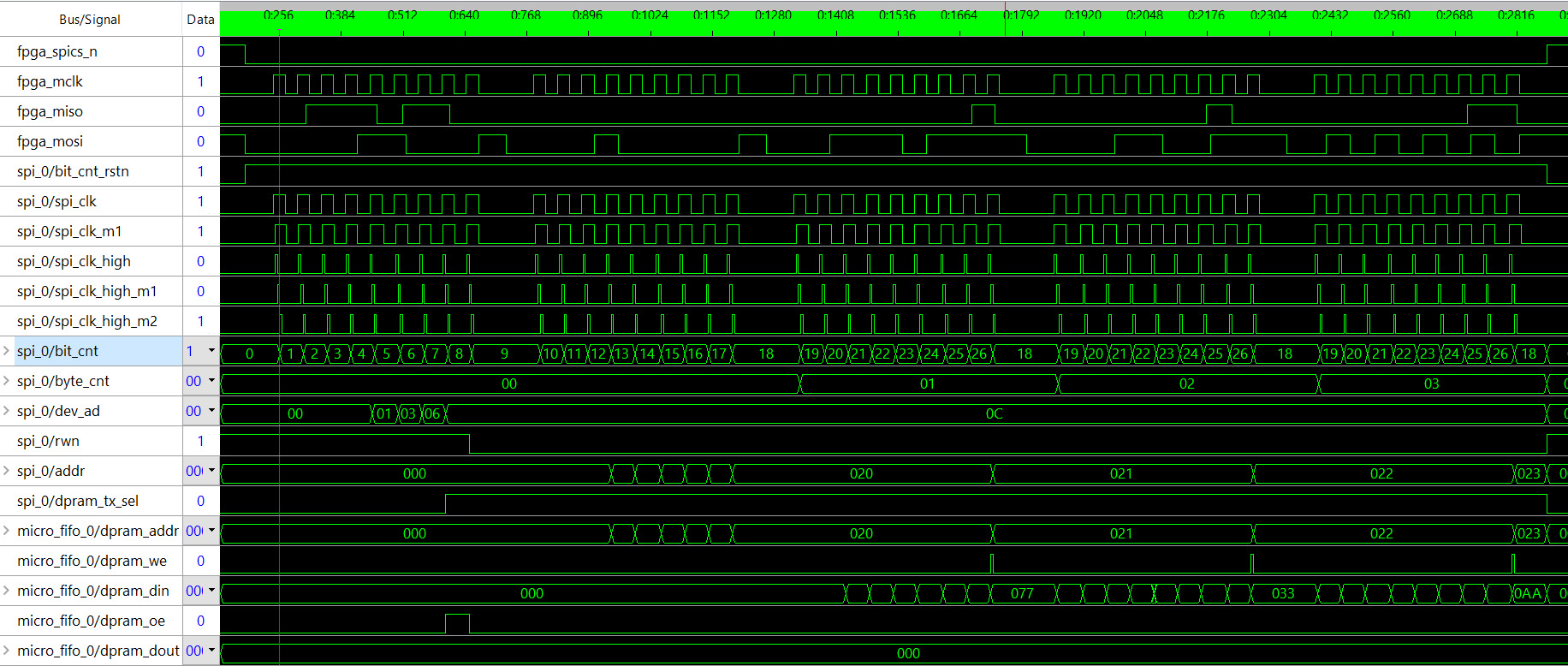
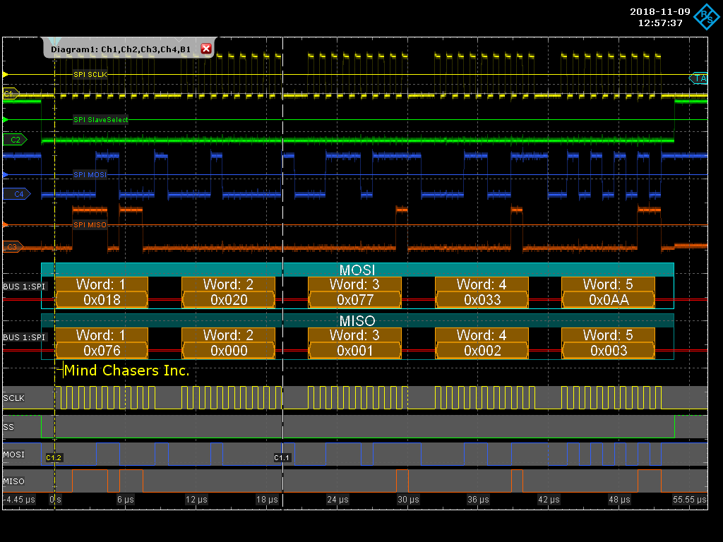
Figure 2 shows a Lattice Reveal Logic Analyzer screen shot for a three word data write cycle from the K02 to the FPGA. This trace shows the top level SPI signals and also internal spi and micro_fifo signals. Note that all data is shown in hex format. Figure 3 shows the same transfer using an oscillscope connected to the four-wire SPI bus.
Each SPI cycle starts when the K02 asserts the fpga_spics_n (pcs) signal. This in turn negates the synchronous reset bit_cnt_rstn.
The top level clk_10 clock signal is used to clock all registers within the spi module including the spi_clk clock signal. This is critical since the memory write enable we must by synchronous with the top level timing. Multiple delayed clock enables are created internally (e.g., spi_clk_high) that are used to sample data and assert signals in lock step with each other.
bit_cnt is the primary state variable that is used to determine when to capture and drive data into and out of the multiple shift registers (e.g., dev_ad). Please see SPI Basics and Protocol for a discussion of the high level SPI protocol and the use of the bit count.


Date: Aug. 18, 2020
Author: Chia-Chi
Comment: