Overview
BTC's (Bottom Termination Components) are everywhere. These are the devices with terminations / leads hidden under the package and often have large thermal / ground pads in the center. We use them extensively on all new designs and are continually seeking to develop the best process possible to produce low cost, reliable, high quality solder joints with a low percentage of voiding.
This article reviews a subset of our process and results with Texas Instrument's DP83867CS Gigabit Ethernet PHY device. This device is packaged in a 7 mm2 48-pin QFN package with a 4.1 mm2 thermal pad. For this type of package, we have adopted a methodolology of creating SMD (solder mask defined) windows for the thermal pad. Our in-house CAE tool is Altium Designer, and we build our BTC footprint using their IPC Footprint Wizard followed by manual customizations for the thermal pad and some additional fine tuning of the footprint features. We find that we can quickly build customized BTC footprints in a matter of minutes using this process.
You can read about the SMD Window approach in this "Printed Circuit Design & Fab" article, and the figure below is from the article and is representative of what we're trying to achieve:
*Source: M.Kelly, M.Jeanson et al, IBM Corporation
Our goals for this methodology, which are discussed in the aforementioned article, include:
- Utilize low-cost, open, through-hole vias
- Eliminate solder wicking down the thermal pad vias by blocking it with solder mask windows.
- Use sufficient number of vias to transfer heat from the thermal pad
- Reduce stand-off variability and improve reliability
Create the basic footprint
The basic footprint with a single, monolithic thermal pad is shown in the figure below. Red is copper, and purple is solder mask. In Altium, we set the thermal pad's solder mask expansion to manual and a negative value to eliminate its definition. Remember that the solder mask is a negative image. We'll define the solder mask (windows) in the steps below
Note that some manufacturers still recommend this basic footprint for their BTCs / QFN packages. We consider this a quick and dirty approach. The primary disadvantage with this approach is that solder can run down the via holes during reflow, create shorts on the wiring side, and also impact the quality of the connection to the thermal pad.
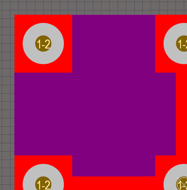
Define a single SMD Window
The upper left SMD window is drawn first using a single polygon region. Before placing the polygon, we perform all the geometry calculations. We strive to keep board cost to a minimum, but we also choose a PCB fabricator that can deliver things like high quality 8 mil drill holes and 6 mil solder mask webbing.
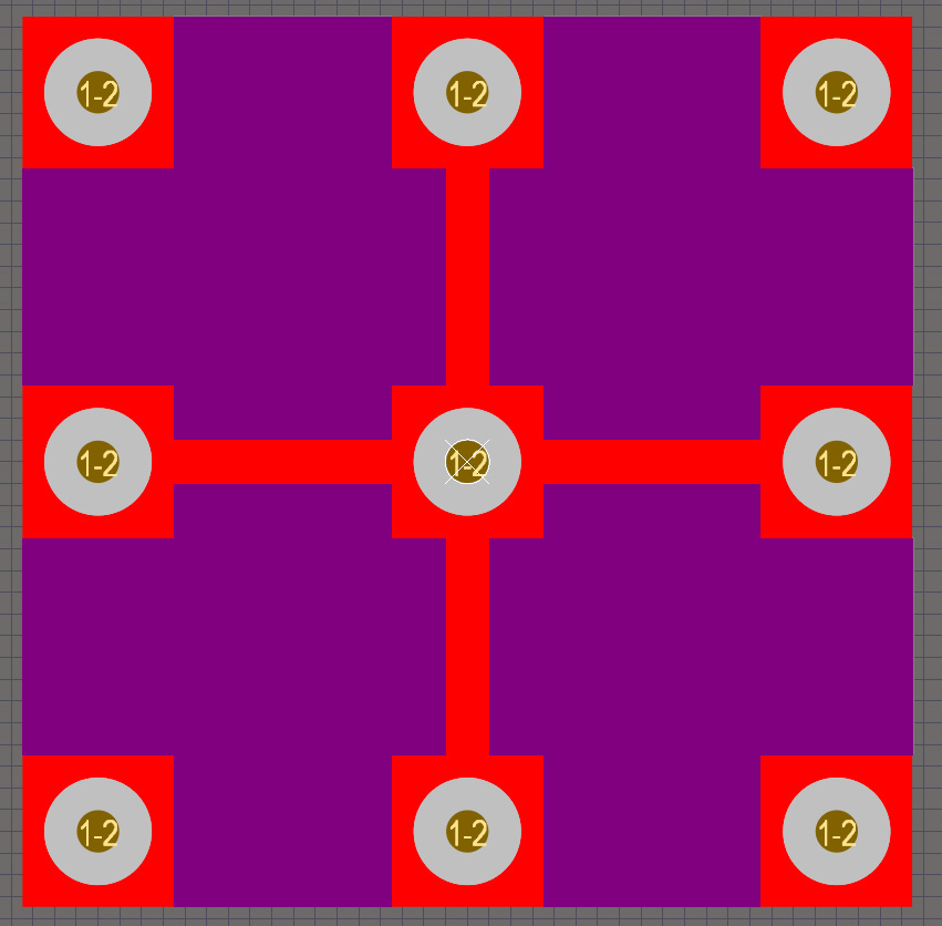
Complete the Thermal Pad Solder Mask Definition
- Copy and paste the upper left SMD Window three times to create the other windows. Use 'X' and 'Y' shortcuts as necessary to flip the windows. Make sure the grid enables positioning each window with perfect symmetry
- Manually set the solder mask for each via, so they are not tented.
- Copy the new SMD window solder paste polygons and paste them on the solder paste layer. Note that you may wish to reduce your solder paste openings.
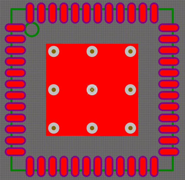
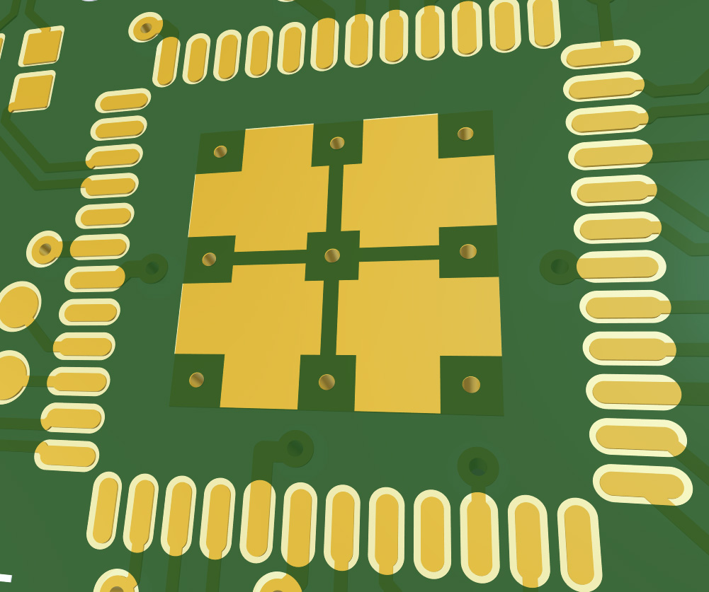
A look at the rendered footprint
After associating the new footprint with the device, the rendered 3D image of the PCB is shown below:
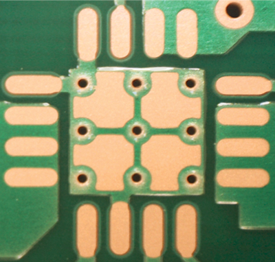
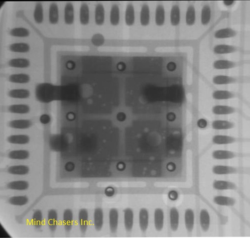
Assessing voiding
The figure below shows an image of the device after reflow using a low voiding paste. We're encouraged by the results but also working to improve the process.


Date: Nov. 11, 2017
Author: Chandru
Comment: