Technology and Engineering Services that enables home owners, businesses, makers, and hobbyists to take control of their network
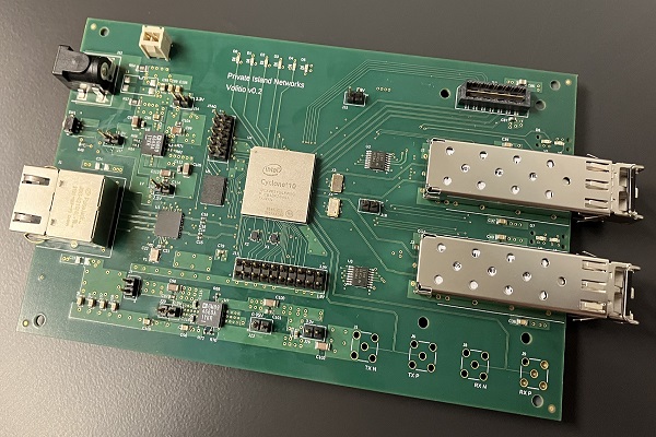
Volitio
10G Ethernet for Private Island

Private Island
Open Source FPGA Network Processor
Coming Soon
GigE Maker Board for Private Island
Private Island Networks Inc.
Design and Manufacture of Custom Networking Systems
Technology to control and trust your network

FPGA to Ethernet SGMII
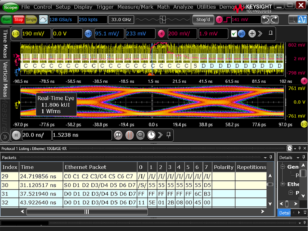
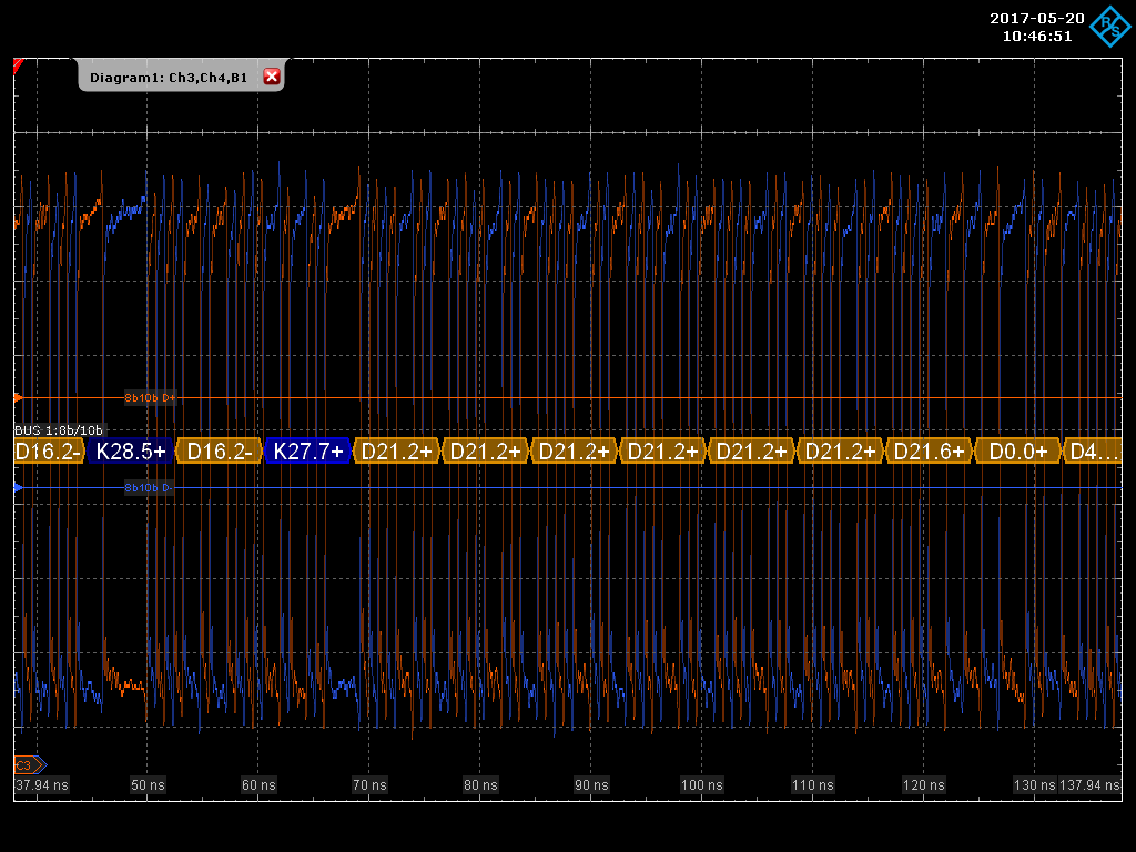
Decoding 10Gb Ethernet
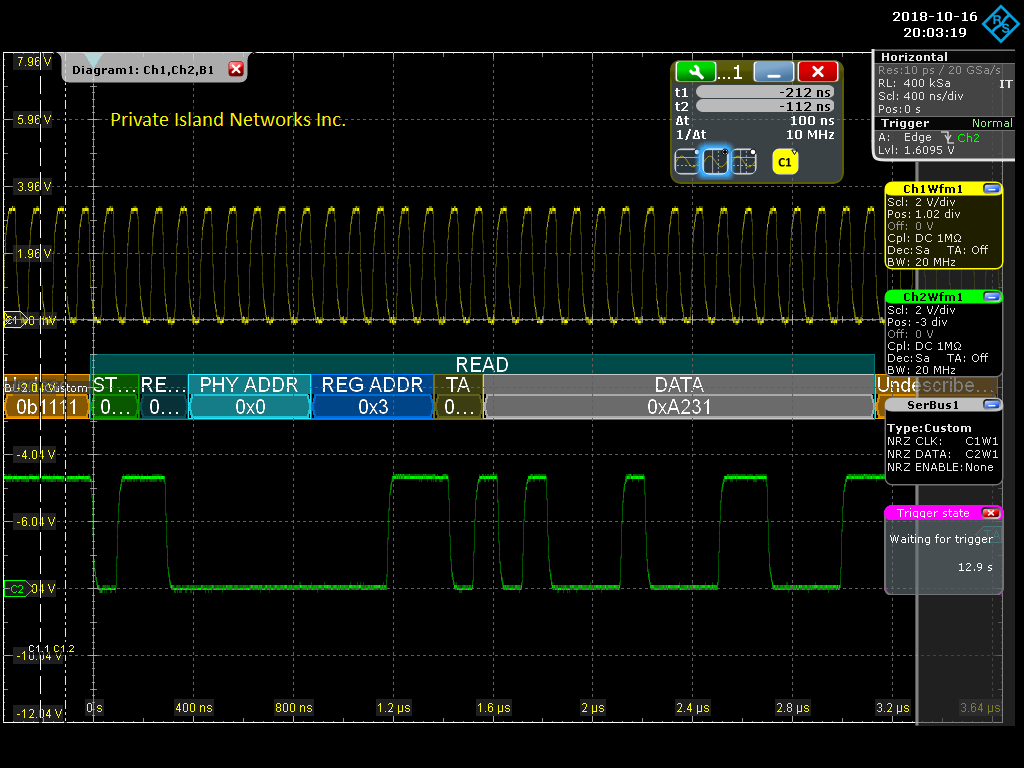
MDIO

