Overview
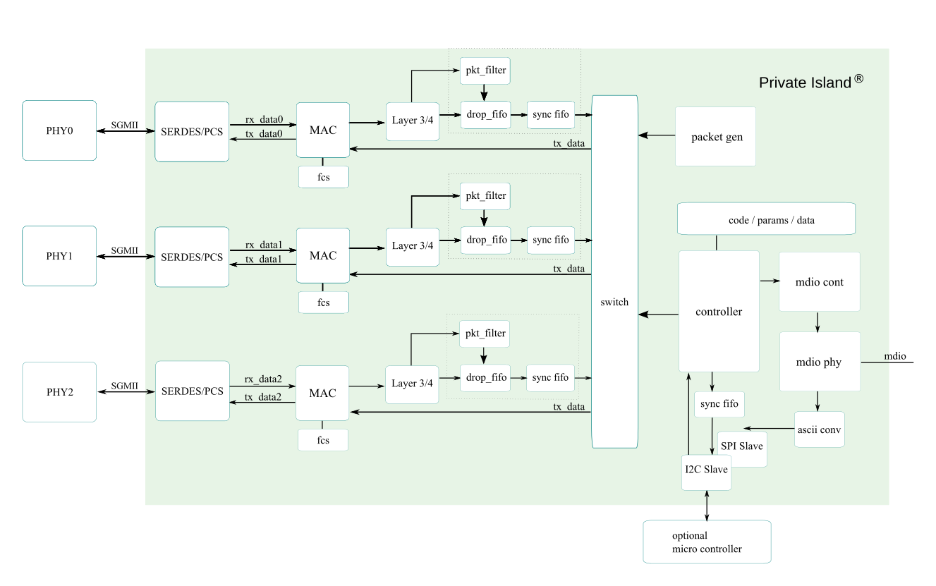
Provided below is draft documentation for the FPGA architecture and Verilog modules that comprise the Private Island ® project. Documentation is being updated on a regular basis.
The source code is hosted here using cgit.
The system is highly configurable, and the user can specify at build time many parameters including the number of PHYs to instantiate, packet filter purpose, trigger points, & size, and buffer depths.
The project currently supports the Lattice Semiconductor ECP5UM and Texas Instruments DP83867 Gigabit Ethernet PHY. An external on-board micro controller is assumed to be present for FPGA configuration and control. Any micro controller can be used, but our development system utilizes an NXP Kinetis K02 (ARM Cortex M4) with the Ethernet MAC for the K02 integrated within the FPGA.
The figure below depicts a system with three PHYs instantiated for the purpose of connecting PHY2 to a local Linux processor. Example usage would be a network tap or a dedicated system controller port for performing higher level packet analysis and control. In this scenario, the Private Island ® system acts as an Ethernet bridge / filter / firewall between PHY0 and PHY1.
Verilog Coding Conventions
- data buses follow a naming convention: dir_driver_function_srcSlot_destSlot (e.g, rx_df_fifo_d_01)
- delayed / registered data: _m1, _m2, _m3, _m4
- K28_5, D16_2 represents 8’hBC, 8’h50, /I2/ or IDLE 2
- FIFOs are used throughout to buffer data
- worker interface definition to start and finish work assigned by internal controller: controller.v
- one shots are common and trigger further action
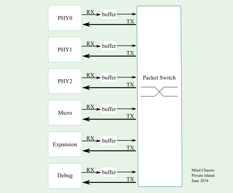
Switching
The figure below depicts the packet flow and high-level switch architecture. The packet switching is centralized and is controlled by configuring the source for each TX port.
Regardless of port, the Receive (RX) direction is always into the switch, and the transmit (TX) direction is always from the switch. Data buffering and filtering / dropping is done in the RX direction.
Currently, all packet data (byte/octet wide) is clocked at 125 MHz . However, it is possible to down sample the data into a wider data path for analysis and storage functions (e.g., 32-bits @ 31.25 MHz).
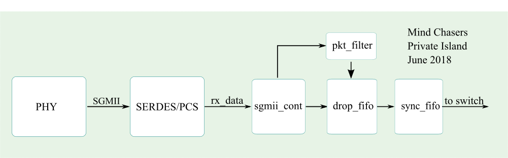
Receive Path
The figure below depicts the packet data receive path. The PHY is external to the FPGA and connects via SGMII. The SERDES/PCS block is a hard macrocell within the ECP5UM. The remaining blocks in the figure are Verilog modules and are described further below.
SPI
See the following:
MDIO Controller
Additional Modules
A partial list of module descriptions is provided below (documentation is being added on a regular basis):
mac.v
Purpose: SGMII TX/RX/AN state machines
- Controller is specific to both SGMII and a lesser extent the Lattice PCS block.
RX notes:
- Each frame written to the FIFO consists of the MAC destination, MAC source, Ethertype, and packet.
- Ethernet preamble and FCS are not stored
- However, the first 2 bytes of FCS are written into FIFO due to a lag issue on stopping a read during TX
- The RX packet complete bit is set on the last RX byte, so two more bytes are written after that (FCS).
- RX data written into FIFO is from rx_data_m1 register
TX notes:
- If code group /R/ is transmitted in an even-numbered position, append a single additional /R/ to the code-group stream to ensure that the subsequent /I/ is aligned on an even-numbered code-group boundary and EPD transmission is complete.
- Reading the FIFO starts two clocks early since data isn't available until after the first clock and then we register the data from the FIFO on the 2nd clock.
- Reading stops (tx_fifo_re is deasserted) after either tx_last_byte or tx_fifo_empty are detected on the next clock, These signals are expected to be coincident.
pkt_filter.v
Purpose: packet filter / CAM wrapper with keep / drop logic
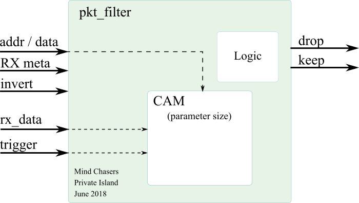
cam.v
Purpose: single cycle, parameterized Content Addressable Memory
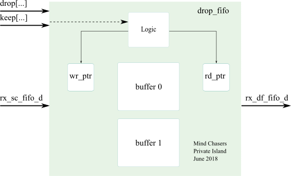
drop_fifo.v
Purpose: Double buffered side-by-side FIFO with keep / drop logic
Notes:
- Writer and Reader may either be active on first or second buffer simultaneously
- Delay (buffer depth) is set outside this module by writer ( hold off of keep or drop )
- A write can't begin on buffer[n] while a read is active on buffer[n].
- This is guaranteed to not happen as long as 2*IPG + tWR > tBuf[n]
- RX data is dropped after drop is asserted ( FIFO wr_ptr is reset ). Read on this buffer is inactive.
- FIFO buffer becomes available again after drop ( no need to switch to other buffer ).
- this lets writer drop packets early without regard to other buffer.
- FIFO is cleared on drop by setting wr_ptr to 0
- There is always a minimum gap between a need to switch buffers: FCS+IPG+PREAMBLE
- There is no empty flag since rd_ptr and wr_ptr may be pointing to different buffers.
sync_fifo.v
Purpose: Buffer RX data until ready for TX switch


